Native Defects Enable Facile Measurement of the Carrier Concentration in Two-Dimensional Semiconductors Using Kelvin Probe Force Microscopy
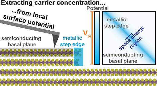
The carrier concentration is an important property of semiconductors; however, measuring the carrier concentration is challenging for nonstandard samples. Here, we report a method for measuring the carrier concentration in 2D semiconductors using sideband Kelvin probe force microscopy. We map the surface potential (1) at three Pt–transition-metal dichalcogenide (TMDC) interfaces and (2) at step-edge defects native to the TMDCs. Mapping the local surface potential across Pt–TMDC interfaces enables quantification of the built-in potential and the space-charge-region width, from which the carrier concentration can be calculated. The calculated values are similar to those obtained from simulations of the 3D space-charge region at Pt–TMDC interfaces. Mapping the local surface potential at step-edge defects in the same crystals and modeling these defects as rectifying metal–semiconductor interfaces yields similar carrier concentrations. Together, this work provides a straightforward, nondestructive method for measuring the carrier concentration in 2D semiconductors.
Chua, K. O.; Leimkuhl, D. P.; Fernandez, P.; Kumbhar, A.; Lopez, R.; Jackson, M. N. Native Defects Enable Facile Measurement of the Carrier Concentration in Two-Dimensional Semiconductors Using Kelvin Probe Force Microscopy. Nano Letters 2026. DOI: 10.1021/acs.nanolett.6c01913